
Designing with Transistors - Chapter 4
4.0. OVERVIEW
So far we have only looked at the voltage divider method of biasing a transistor stage. Now we will look at another method which is simple and economical. These advantages are, however, at the expense of other parameters.
Once we are satisfied with a single stage amplifier, the problem then arises of how to connect this into the system so that it does not disturb the driving or driven circuits. Sometimes direct coupling is possible but often we must make use of a d.c. blocking capacitor. The value of this component must be such as to maintain the required bandwidth (frequency response) of the system.
4.1. ALTERNATIVE BIASING ARRANGEMENT
There is an alternative to the R1, R2 divider known as "collector to base feedback bias". Only one resistor is needed instead of two and some bias stability is possible even without the inclusion of RE; (see Fig. 4.1). The resistor Rb provides bias and also some negative feedback which tends to stabilize the collector current against changes in hFE.
Suppose that hFE is higher than predicted: this would tend to increase Ic which in turn would cause the output voltage to fall. this fall would be passed via Rb to the base causing a decrease in Ic. The base bias conditions are therefore stabilized.

HIDDEN FEATURES
Although the method appears delightfully simple and economic, there are certain hidden features which the designer must understand:
-
The feedback is in parallel with the input signal and therefore requires extra current drive from the signal input to the stage. In other words, the stage input resistance RIN is lowered. In fact, the input resistance consists of two resistors in parallel, one of them being the normal rIN = hfe * re and the other equal to Rb divided by the gain A.
This is easily understood when it is realised that the signal voltage is at one end of the Rb and the output voltage (A times the input signal) is at the other. -
Thus A times as much current must be provided by the signal, which is equivalent to saying that Rb behaves as if it were A+1 times smaller and across the signal input.
-
There is no actual reduction in voltage gain, as far as the gain from base-in to collector-out is concerned. The voltage gain is still
A = Rc/re or Rc/(re + RE) (If RE is present).
However the lower input resistance has the effect of lowering the gain measured from signal e.m.f. to collector output. (see Fig. 4.2). If A was. very high, the total gain from Vs to Vout would be approximately A'=Rb/Rs where A' is defined as the gain with feedback. Thus the gain is independent of the transistor.
This, however, is a gross over simpfification of the situation because the transistor gain A in such a simple single stage ampli6er would not be "very high" and A' = Rs/Rs would be greatly incorrect.
4.2. AN ALTERNATIVE EQUATION FOR GAIN
The previous circuit had no emitter resistor RE which was the reason why the gain A was so high. Although a high gain may often be a desirable feature there are two main reasons against achieving it by the omission of RE.
-
The gain is not too predictable because of its absolute dependency on re. The equation re = 25/Ic(mA) is very useful as a rough guide but it is well to remember that the equation is only approximate. The inclusion of RE in the gain formula, although lowering the gain increases the accuracy of the equation (particularly if RE » re).
-
A more important reason is the rather remarkable twist of the gain equation when the bias is set to allow the collector to rest at half the supply voltage.
if Vout = ½ Vcc then Rc = ½ Vcc/Ic
Now A = Rc/re = (½ Vcc/Ic) ÷ (25/Ic )= Vcc/50
But remembering that the figure '25' is in millivolts, we must. multiply by 1000, giving
A=(Vcc*1000)/50 thus A=20Vcc
This means that the gain of any grounded emitter stage operating without an emitter resistor is simply 20 times the supply voltage (assuming the collector is at half the supply voltage). This applies whatever collector current we use, so it is impossible to set the gain at any other value than 20 (unless of course we use negative feedback). It is easy to see why RE is almost always present in grounded emitter amplifiers.
4.3. COUPLING CAPACITORS
It is often required to connect two stages together by allowing the output signal of one stage to become the input signal of the next. Sometimes the coupling can be achieved without disturbing the d.c. bias conditions, but this is sometimes unavoidable. This problem can be overcome with the use of a "coupling capacitor" which enables the signal to pass relatively easily but blocks any d.c. from affecting the next stage.
CAPACITOR VALUE
The question is how big must the capacitor be? The answer depends on two pieces of information.
The lowest frequency that the signal is likely to be, and the input resistance of the stage which the capacitor is to feed.
The skeletal circuit is shown in Fig 4.3.
The capacitive reactance (Xc) and RIN form a voltage divider, so it is clear that Xc should be considerably less than RIN at the lowest frequency which it is desired to pass.
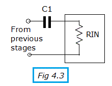
The simplest way is to find the value of C which makes Xc = RIN and then use the next highest preferred value.
Suppose the lowest frequency to be passed is 100Hz and RIN = 1kΩ Then if Xc = RIN then 1/(2 Π fC) = RIN which gives C = 1/(2Π f RIN) Inserting values gives C = 1.59µF so the next highest preferred value, 2µF would be used.
RULE OF THUMB
A neat little rule of thumb to save a lot of fiddling with powers of ten is
C = 0.2/(f * RIN)
where f is in kHz, RIN in kΩ and C is in uF.
The value for C is in no way critical, providing it is at least the value calculated by the method above. Twice or even ten times larger will not matter apart from the cost.
4.4 USE OF THE EMITTER FOLLOWER STAGE
An emitter follower stage provides an easy solution to the problem of matching from a high resistance signal source to a low resistance load. Unlike the normal grounded emitter stage, the emitter follower has no voltage gain, in fact, there is a slight voltage loss.
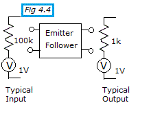
There is, however, a substantial current gain as a signal is passed through, because of the apparent change in source resistance. Treating the emitter follower as a black box, the effect on the input signal is as shown in Fig. 4.4 The values shown in the figure are purely arbitrary and are chosen only to illustrate how the source resistance can be substantially lowered by passing through the stage.
CURRENT GAIN
The concept of current gain can be appreciated by calculating the two short circuit currents. If the original circuit was shorted out the current would be I = 1V/100k = 0.1mA If the output was shorted, the current would be I = 1V/lkΩ = lmA.
This shows that a theoretical current gain of 100:1 has been achieved. (The short circuit current dodge is used on paper only - don't take it literally and start sticking screwdrivers across the terminals.)
It must not be supposed that an actual emitter follower would provide a magical solution. The successful design of such a stage requires quite a bit of fiddling with values to get the input resistance as high as possible.
For example, Fig. 4.4 presupposes that the input resistance of the emitter follower stage is much higher than the 100kΩ signal resistance. Unless this is so, it is clear that the signal would be attenuated by voltage divider action between the 100k and RIN of the emitter follower.
An emitter follower circuit using voltage divider feed for base bias is shown in Fig. 4.5.
We are not concerned with the design factors for setting up the correct d.c. conditions, this problem is dealt with elsewhere. Instead, we state some important equations which decide the voltage gain, input resistance and output resistance.
1. VOLTAGE GAIN
For most practical purposes, the voltage gain is nearly unity, though it is as well to know the following formula in case some badly chosen values for RE lower the gain to a small fraction
Voltage gain from Vin to Vout = RE/(re + RE)
Since re is the true internal emitter resistance and will seldom be in excess of 100Ω or so, it it easily seen that the gain will be about 1, providing RE; is in excess of 1k.
2. INPUT RESISTANCE (Rin)
This is the same basic formula which has already appeared in connection with the grounded emitter stage.
RIN = R1, R2 and rin in parallel
fe(re + RE).
3. OUTPUT RESISTANCE (Rout)
This is a bit complicated unless dealt with in two parts.
Rout = Rs/hfe in parallel with RE where Rs = R1,R2 and rs in parallel.
If this is too wearisome to calculate and a very rough equation is all that is needed, then use
Rout = rs/hfe

4.6 D.C. COUPLING
Two stages may be coupled together directly only if the dc voltage of the first stage
is compatible with the d.c. bias requirements of the second-stage.
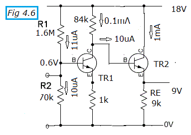
A typical example which serves to illustrate the system is the circuit of Fig. 4.6 which shows a normal grounded emitter amplifier feeding an emitter follower stage.
Transistor TRl provides the voltage gain and TR2 provides a low-resistance (higher current) output.
The gain of the first stage = Rc/(re + RE) = 84k/(1k + 250) = 67
The second stage contributes no further voltage gain.
STAGE INPUT RESISTANCE
The stage input resistance is rin, R1 and R2 all in parallel although it is reasonable to ignore R1.
Now, rin = hfe(re + RE) = 100(250 + 1k) = 125Ω which in parallel with with R2 gives a value for RIN of about 45kΩ
Currents-through TR2 would be determined first. 1mA is chosen for collector current, so assuming a pessimistic hfe of 100, the base current of TR2 would be 10µA.
The divider feed for the bias of TR2 is the chain Rc, TR1 and REof the first stage which is passing 0.1mA (which is ten times the base current of TR2). Again taking an hFE of 100 for TR1, the base current would be 1µA; which is fed by a divider chain taking 10µA The "rule of ten" has thus been used throughout.
OUTPUT RESISTANCE
The output resistance of the emitter follower is a bit tricky The equation, as stated previously, is
Rout = Rs/hfe in parallel with RE.
The term Rs is the source resistance of the signal feeding the base which, in this case is the output resistance of the first stage. To a rough approximation this may be taken as the collector resistance, Rc which is 84kΩ. Thus Rout =84k/100 = 840Ω (the 9kΩ RE which strictly is in parallel may be disregarded )
4.7 D.C. FEEDBACK LOOPS
The circuit, including the voltages and currents are exactly the same, apart from the method of biasing the first stage: instead of the customary divider across the supply rail, the bias feed a taken from across the output resistor.
This is not such a violent change as appears at first sight. After all, there are nine volts available so why not use them and obtain. the added advantage of a d.c. feedback loop.
In choosing the values For R1 and R2 we must be careful not to disturb the output circuit too much. It is drawing 1mA so it will hardly be aware of the theft if we divert say 10µA from RE to feed a divider.
Since R2 must drop 0.7V, R1 must drop the retaining 8.3V which means that if 10µA is flowing the values of R1 and R2 are calculated as follows:
R1 = 8.3V/10µA = 830kΩ
R2 = 0.7V/10µA = 70kΩ

STABILITY
Such a circuit has very good stability in spite of wide tolerances in the resistors R1 and R2. In fact, it is astonishing how the output appears to lock at 9V. Suppose that the output tends to drift downwards: this will pull the base of TR1 down which causes the collector of TR1 and base of TR2 to rise. The output tendency is therefore to rise which. due to the feedback loop is providing a correcting influence on the tendency for the input to fall. The original gain before feedback is of course, reduced from its previous value. This is one of the penalties ta be paid for the benefit of negative feedback.